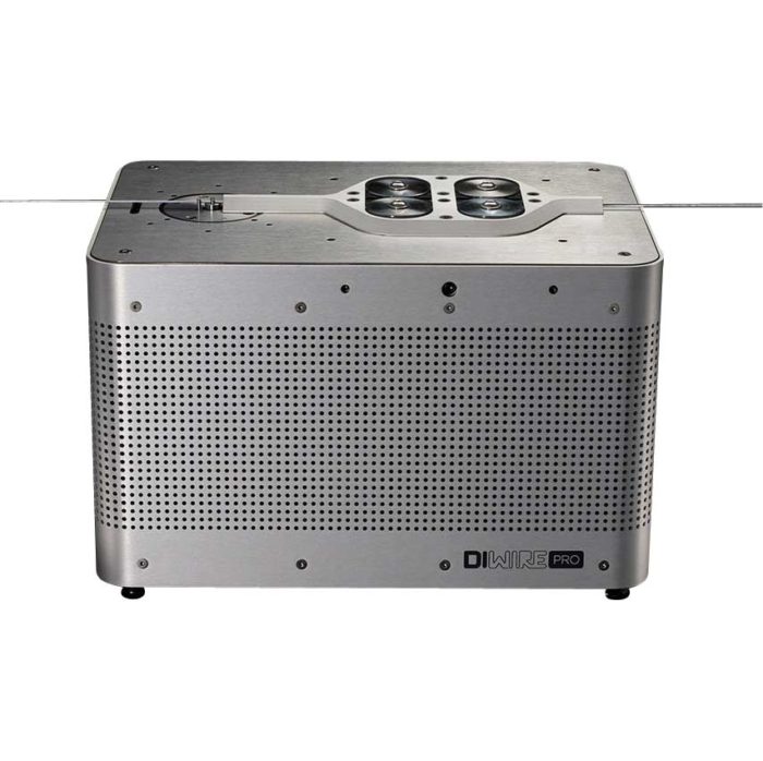
A wire former with precision and power
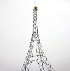
The newest CNC benchtop wire former by Pensa Labs, offers the kind of power, speed, and precision that professionals need. Fully configurable and affordable, the D.I.Wire Pro solves your prototyping or small batch production needs. The machine has a bend mechanism that delivers smooth, tight radius curves, accurately and with repeatable results.
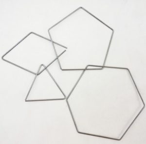
Accuracy, precision and repeatability
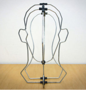
Whether you need thousands of the same part or hundreds of unique parts, the D.I.Wire Pro machine is able to help you maintain accuracy, precision and repeatability. The machine is configurable to all your wire bending needs and can be equipped with an automatic cutter and wire straightener to increase productivity.
Request a Quote
What can the D.I.Wire PRO do for you?
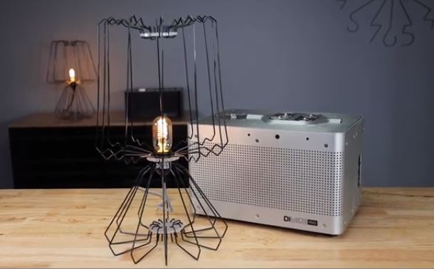
The newest CNC wire bender, offering the kind of power, speed, and precision that professionals never thought possible from a bench top machine. The D.I.Wire PRO bridges the gap between time-consuming hand-bending and expensive large-scale, mass production CNC wire bending.
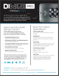
Technical details
Maximum bend angle: 135°.
Wire diameters: 0.063″ (1.6mm) or 0.125″ (3.2 mm).
Feed accuracy: +/- 0.008″ (0.2mm).
Bend pin accuracy: +/- 0.5°
Additional info
Dimensions: 16.25” x 11.25” x 13” (41 x 29 x 33 cm)
Weight: 100 lbs (Shipping Weight: 125 lbs)
Operating Temperature: 15-30°C, 59-86°F
Power Requirements: 100-240 V, 1.8 A, 50/60 Hz
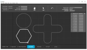
Controlled by Wireware 2.0
The D.I.Wire Plus comes with its own smart bending software, Wireware 2.0. The software is easy to use and allows for high level of control when needed.
Wireware 2.0 offers two ways to produce bent shapes: In Path mode, graphically create shapes or import SVG files. In Script Mode, create complex programs using conversational script or G-code.
Essentials:
- PC with internet access
Recommended:
- Consumables bundle
- 6ft table space
- Diwire Support Plan
Basics:
- Machine set-up and operations (~1-2 hrs)
- Wireware 2.0 essential creations (2-4 hrs)
Advanced:
- Advanced wire bending design (6 hrs)
- For applications and project ideas:
- AET Labs custom lesson plan